ASML High NA EUV system begins arriving at Albany NanoTech
Published
The first major components of an ASML High NA EUV lithography system have arrived at NY Creates’ Albany NanoTech Complex, marking a major step toward ...
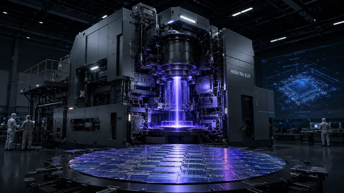
The first major components of an ASML High NA EUV lithography system have arrived at NY Creates’ Albany NanoTech Complex, marking a major step toward establishing North America’s first accessible research center for the technology.
What arrived in Albany
NY Creates received the bottom main module of the ASML TWINSCAN EXE:5200B system. Additional components are scheduled to arrive throughout the summer, with installation and initial development milestones expected by the end of 2026.
Why High NA EUV matters
High numerical aperture extreme ultraviolet lithography uses advanced optics and laser-driven plasma light to print smaller and more complex patterns on silicon wafers. The technology is intended to support future processors with greater computing power, lower energy use and denser transistor designs.
A shared research facility
The system will be installed at the NanoFab Reflection facility inside the Albany NanoTech Complex. Unlike equipment reserved for a single chipmaker, the center is designed to give industry and academic partners access to High NA EUV research and development capabilities.
Investment and partners
New York State says the project is backed by a $1 billion public investment that is leveraging $9 billion in industry funding. Partners connected to the Albany semiconductor ecosystem include ASML, IBM, Micron and Tokyo Electron.
Scale and delivery
The complete lithography system is comparable in size to a double-decker bus and weighs more than 200 tons. Its components are being transported in 250 crates using more than 40 containers, five cargo aircraft and 20 specialised semi-trucks.
When research is expected to begin
The High NA EUV system is expected to begin supporting research and development activity in early 2027. The facility will focus on advanced chip patterning, process development and device scaling, including work related to sub-1-nanometer semiconductor technologies.
Practical significance
Advanced AI systems depend on increasingly powerful and energy-efficient chips. Making High NA EUV available in a shared U.S. research environment could help laboratories and chip companies test manufacturing techniques before they reach full commercial production.
New York State announced the arrival in an official press release .
Source: New York State Governor’s Office